The Next-generation Photomask CD-SEM, “HSS-1000,” was released in November 2025 and construction of our subsidiary HOLON’s new factory was completed in December. A&D HOLON’s semiconductor-related business is steadily advancing to achieve our ‘Long-Term Vision 2034’.
In this special feature, we introduce our new product, the “HSS-1000,” and the new factory of our subsidiary HOLON.
Amazing Features of New Product: “HSS-1000”
New Arrival
Accurate and quick “measurement” technology is advancing at the nano level
A semiconductor is much like a switch that can “allow or block” the flow of electricity. There are actually hundreds of billions of these switches just in the smartphone you use every day, for example. To ensure that each and every one of them functions correctly as a matter of course, technology which measures with both accuracy and speed is indispensable-technology which is imperceptible to the human eye.
A&D and HOLON Combine Technical Expertise!
The “HSS-1000” was designed with an eye toward the standards required in semiconductor manufacturing facilities 10 years from now
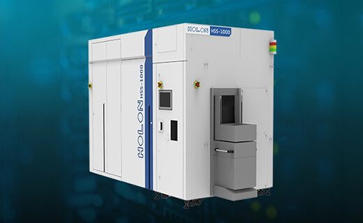
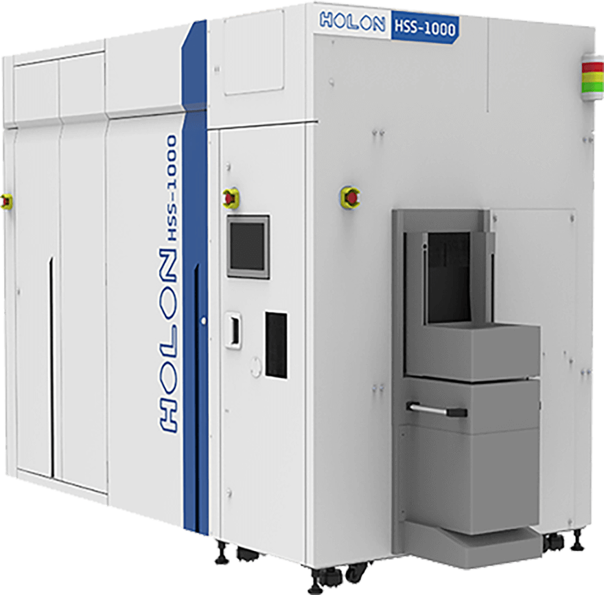
Next-Generation Photomask CD-SEM “HSS-1000”
The HSS-1000 offers significantly improved performance over the previous ZX model, achieving the extremely high dimensional measurement accuracy required for EUV mask manufacturing in the 1.6 nm node and beyond. It is capable of acquiring clear, high-resolution images of thin-film absorber layers (*1) and photoresist patterns (*2). This significantly helps improve efficiency during the mask development phase and improve yield in mass production process.
*1: A thin film on the photomask that absorbs EUV light during exposure, preventing it from reaching the wafer. Areas without the absorption layer reflect EUV light and are exposed.
*2: A photosensitive material applied to a substrate when creating the circuit pattern for a photomask. Its properties change when exposed to light, and fine patterns can be formed through development.
CD measurement accuracy (Static)
25% UP!
Measurement time (MAM time)
30% UP!
Beam resolution (Sharpness)
15% UP!
Contrast to Noise ratio (CNR)
15% UP!
PICKUP!
Some of the Amazing Features
Achieved even higher image resolution and stability!
New design
High-resolution images capture microstructures at the nanometer level with exceptional clarity and three-dimensional detail. By leveraging AI technology, we have achieved even higher resolution and greater stability.
Significant improvement in measurement accuracy!
The dimensional measurement accuracy of the HSS-1000 has been increased by 25%, a significant improvement compared to the previous ZX model, achieving the extremely high accuracy required for EUV mask manufacturing in the 1.6 nm node and beyond. That level of measurement accuracy is equivalent to measuring the distance between Tokyo and London with a margin of error of just 1 millimeter.
They aren’t just smaller! Their processing speeds are faster. Plus, they’re more environmentally friendly.
Semiconductors are what enable the performance enhancements of all kinds of devices, from smartphones and computers to automobiles. In recent years, driven in particular by the widespread adoption of AI, demand for high-performance semiconductors has been growing rapidly. Semiconductors offer significant advantages as they become smaller.
For example, if the circuit dimensions are halved…
Faster
Processing speed Approx.
2x faster
More energy-efficient
Power consumption Approx.
1/4
Miniaturization makes it possible to create semiconductors that operate “faster” and “more energy-efficiently”!
To improve performance, more semiconductors must be packed into a limited space. At the same time, heat generation and power consumption must be minimized as much as possible. It is precisely to resolve these mutually exclusive issues that efforts are being made to miniaturize semiconductors.
The main reason semiconductors keep getting smaller is to achieve performance improvements and energy efficiency at the same time.
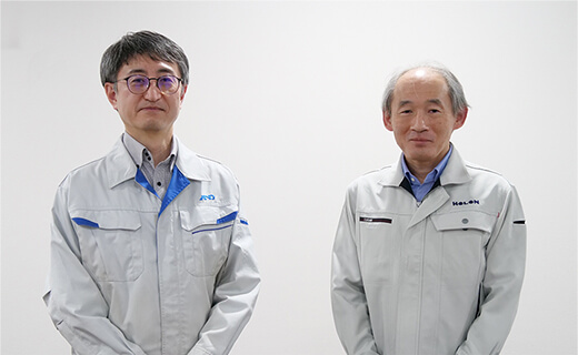
Interview with A&D and HOLON Developers: Insights
A&D Company Limited
Deputy General Manager Semiconductor R&D Department Semiconductor Business Division
Kenichi Katayama
HOLON,co.,Ltd
Director New Technology Business Division 1
Tatsuro Goko
The Battle Against Inherent “Noise”
Mr. Goko
With this new product, our top priority was ensuring the highest possible measurement accuracy. The scanning electron microscope and its control electronics—the core components of the HSS-1000—are not merely an upgraded version of previous models; we developed them from the ground up by integrating the technologies of HOLON and A&D. To achieve the extremely high dimensional measurement accuracy required for next-generation process nodes, we focused our development efforts on improving resolution and signal-to-noise ratio.
In the semiconductor industry, even the slightest deviation directly impacts quality, cost, and production efficiency. That is precisely why customers’ demands for “more accurate measurements” are becoming stricter every year.
Mr. Katayama
The key challenge in achieving accurate measurements was how much noise (*) we could eliminate. When we observed the pattern on the mask using an SEM (Scanning Electron Microscope), initially the image was distorted due to noise generated somewhere inside the instrument.
I stood beside the equipment constantly asking myself, “What could be causing this?,” “Let’s look here next,” as I systematically went through them one by one searching for the source of the noise. * Noise: A general term for unwanted elements that disturb the natural signal pattern.
Mr. Goko
What’s more, there wasn’t just one instance of noise. As soon as we eliminated one, another one came up. To be honest, it felt like a battle with no end in sight.
However, we were determined to create beautiful images. Focusing on the signal-to-noise ratio—in other words, how much we can make the “actual information we want to view” clear and how much we can reduce the “distracting information”—was the key to improving accuracy, I think.
Mr. Katayama
Right! It was that situation when I had to really put my skills as an engineer to the test.
When the image became clear and stable and I was certain we had something we could use, that was the most rewarding moment of this development project.
Results of Technological Synergy Made by Group Structure
Mr. Goko
Outsourcing development could lead to technological assets accumulating outside the company. By entrusting development to A&D, we have established a structure that allows us to retain technical assets securely within the group and also ensured a high level of confidentiality.
I think the major difference from this development being within the A&D HOLON Group was being able to discuss things openly while sharing our objectives and goals.
Mr. Katayama
Being part of the same group, we were able to examine HOLON’s current models firsthand, verify their applications and characteristics, and gain a deeper understanding of them. The time from receiving feedback to making improvements was also extremely fast.
HOLON has unparalleled technology and expertise in handling the electron beam itself and has established a strong brand presence in the photomask measurement field. Meanwhile, A&D possesses world-class technology for controlling the direction of electron beams and has also refined its high-precision measurement control and sensing technologies.
I think our respective strengths came together and were able to complement each other’s deficiencies in this development project.
Combining Group technological expertise to make Japan’s future bright
Mr. Goko
We aim to become a leader in the semiconductor equipment industry about which users say, “We can only see it with HOLON’s equipment”.
To become that leading company, research and development will be key. Rather than reacting to our customers’ challenges, we will proactively invest, secure and develop talent, and further strengthen collaboration within the group. We will move forward to build this kind of structure.
Mr. Katayama
Adopting cutting-edge technology represents a significant investment for customers in the semiconductor industry. In the past, well-capitalized foreign companies have been proactive in this area, while Japanese companies have tended to lag behind.
However, the situation has been changing in recent years. More and more companies in Japan are getting serious about investing in cutting-edge technology.
A&D and HOLON have joined forces and already started work on the next product development. The semiconductor industry is a vital sector that underpins the future of society. With our business, we hope to make a brighter Japan.
Manufacturing Is More Than Just Making Things?!
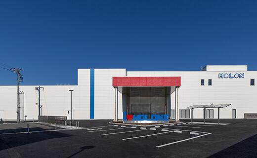
New Factory
HOLON’s factories don’t just build things; they also build trust
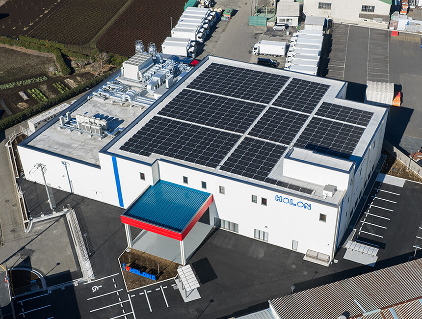
New HOLON Factory (Completed: December 2025)
Address:
4-55-7 Ichibancho, Tachikawa City, Tokyo
Area:
Site area: 4,602.64 m² / Total floor area: 4,241.79 m²
HOLON Main Factory
Address:
5-40-1 Kamisunacho, Tachikawa City, Tokyo
Area:
Site area: 2,847.72 m² / Total floor area: 4,584.40 m²
POINT01
Production capacity has significantly increased!
Production has increased, driven by growing global demand for semiconductors, and product development intensified, spurred by technological innovation. In less than a year after moving to the new main factory,
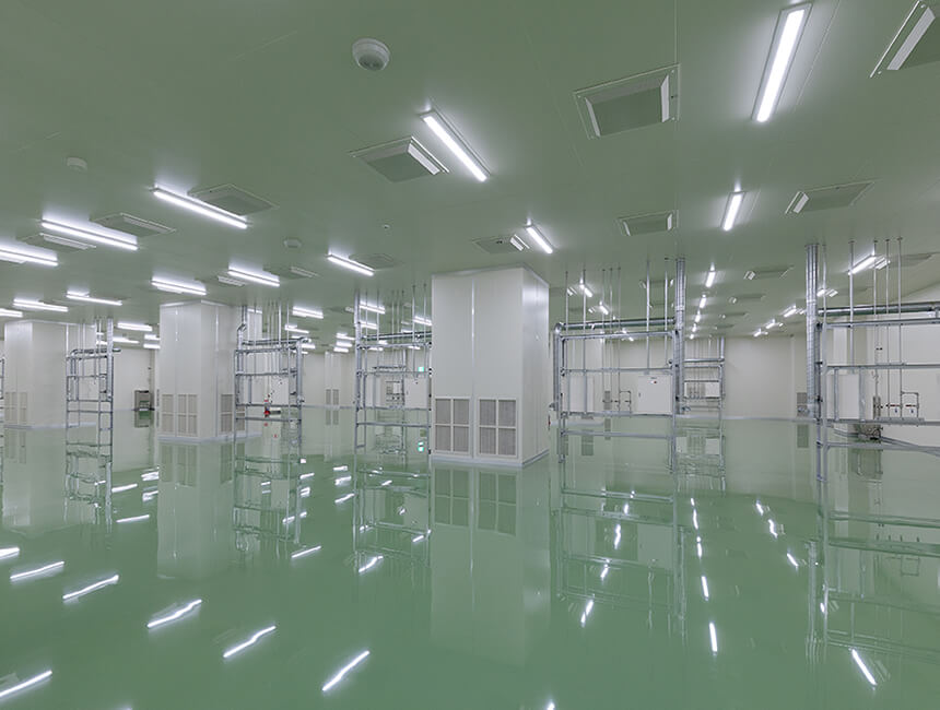
the cleanroom had already become too small due to an increase in development and demonstration units.
We have established a new factory to meet this increase in orders and expanded development. Its cleanroom has been expanded significantly compared with the main factory, ensuring we will also be able to meet increases in demand in the future.
POINT02
“Closeness” Between Development and Manufacturing
While web meetings are convenient, the benefits of the R&D and manufacturing teams being able to discuss matters face-to-face while examining the actual equipment are significant.
We consolidated manufacturing operations at the new factory, while the cleanroom at the main factory nearby is now used primarily for development purposes.
The new factory is located about a 10-minute walk away. It will consolidate equipment and personnel to serve as a facility dedicated to manufacturing, while the cleanroom at the main factory—which was previously used for manufacturing—will primarily be used for development, with some shared use for demonstrations.
This is helping us optimize and expand our product development. We are working on multiple development projects at the same time at our main factory. Another major advantage of the new factory is its close proximity to the main factory. Despite web meetings being convenient, when a problem arises, the manufacturing and R&D teams can meet face-to-face at the factories and have discussions while checking the actual equipment. This “closeness” leads to further enhanced production speed and quality of the equipment.
POINT03
Superior service builds greater trust from customers worldwide
Some customers even place an order without a demo
HOLON’s equipment operates all over the world, 24 hours a day, 365 days a year. In the event of an issue occurring, aside from remote support, they will immediately send a technician to the site, wherever in the world.
Even without having made any aggressive sales pitches, we sometimes receive orders from customers who say, “We’d like to go with HOLON,” without even seeing a demo. The reason for this is simple: we offer comprehensive support and are highly trusted. Our customers recognize our track record and the trust we have built up over the years. Furthermore, going forward, our service representatives will share the “users’ voices” they collect with the R&D team at our main factory and we will proactively develop “the next equipment our customers will need” with our customers’ investment plans in mind.
POINT04
Enhanced procurement capabilities through business integration
A single HOLON device contains a vast number of parts. To maintain stable production, it is essential to continually grasp market supply conditions, prices, and delivery schedules, and to procure materials in a planned and systematic manner. In recent years, rising prices have led to an upward trend in component costs, posing a risk of squeezing profits. To address these challenges, HOLON works closely with A&D’s procurement department to strengthen the Group’s procurement structure and network, thereby ensuring stable and efficient parts procurement.
HOLON’s factories don’t just build “products”; they build “trust”. By integrating our development capabilities—which capture customer needs—with our manufacturing capacity to meet demand, our comprehensive support and service, and our stable procurement capabilities, we aim to “remain a globally trusted company.” Factories have much to contribute in realizing these things.
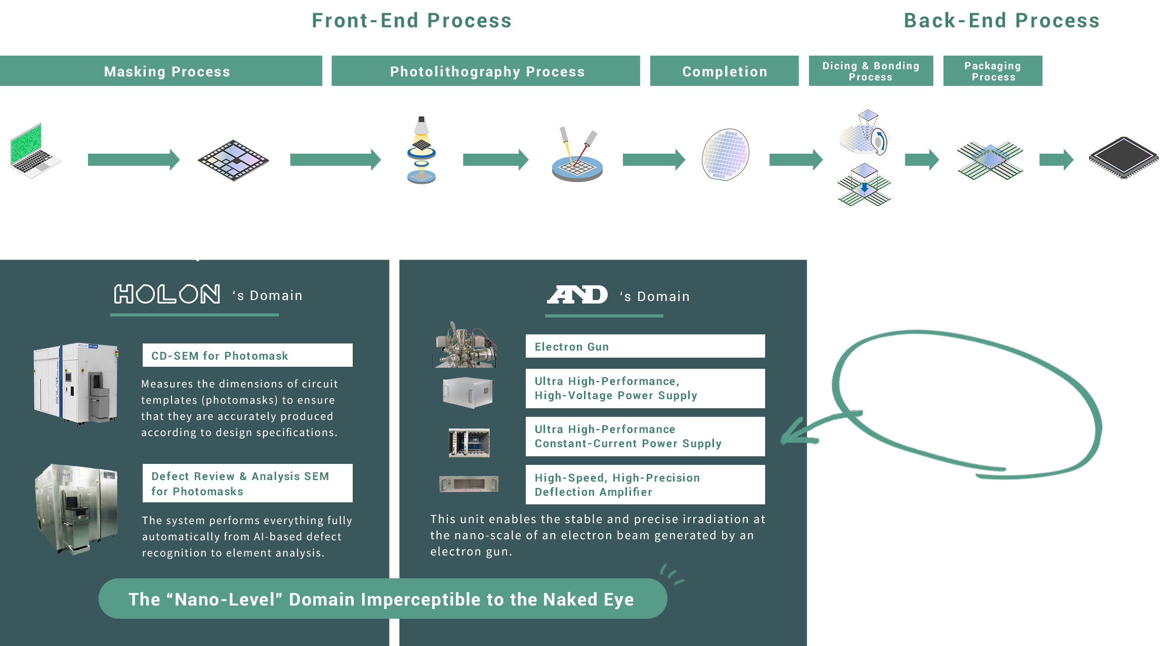
A&D HOLON’s Process Technologies for Semiconductor Manufacturing
Where A&D HOLON Technology Is Used
Our measurement technology is used in the “mask process,” often referred to as the “heart” of semiconductor manufacturing because it is such a critical process.