Shareholder
Communication


TOP MESSAGE
We would like to express our sincere gratitude to our shareholders for their continued support.
Here we will report our financial results for FY2023/24 Q2.
Both sales and profits exceeded forecasts
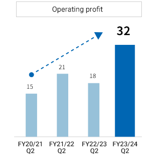
Semiconductor-related Business grew significantly, driving overall operating profit.
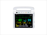
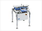
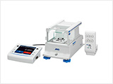
For our Semiconductor-related Business, orders remained firm, with no backlog delays, and both manufacturing and shipments were able to meet customer demand, resulting in a significant increase in sales compared to the same period of the previous year. In terms of profits, improved productivity and cost reductions through group procurement resulted in a significant increase compared to the same period last year, driving overall operating profit. In our Medical and Health care Equipment Business, sales remained on par with the same period of the previous year, and demand for home blood pressure monitors remained strong, especially in the U.S., contributing to both sales and profits. By contrast, in our Measuring and Weighing Equipment Business, despite steady sales progress in Japan, sales and profits decreased due to the impact of the reactionary decline from the previous fiscal year for special demand of mainstay Weighing Equipment in the Americas and sluggish capital investment demand for measurement, control, and simulation systems (DSP systems).
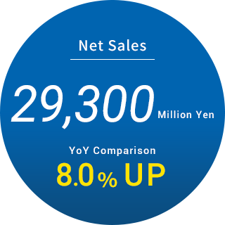
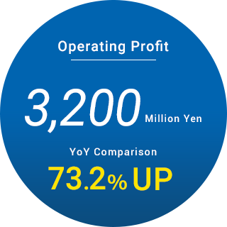
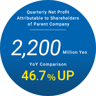
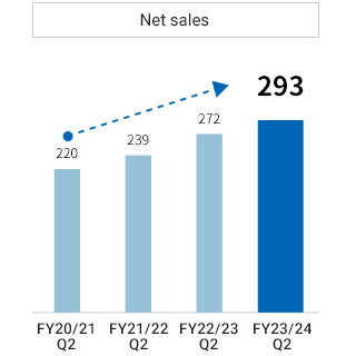
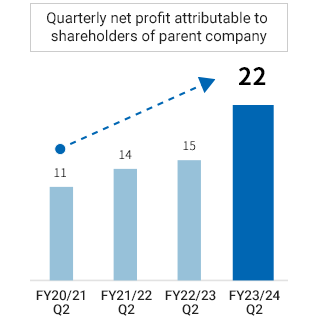
As a result, net sales were 29,335 million yen (8.0% increase year-on-year), operating income was 3,163 million yen (73.2% increase year-on-year), ordinary income was 3,411 million yen (52.8% increase year-on-year), and net profit attributable to shareholders of the parent company was 2,150 million yen (46.7% increase year-on-year).

Business Results Forecast for FYE March 31, 2024Both sales and operating income are expected to increase when compared to the previous fiscal year.
The future of our business environment remains uncertain due to factors such as heightened geopolitical risks, concerns about rising global inflation, economic recession, and the impact of exchange rate fluctuations.
However, we will continue to view the changes throughout society and industry as an opportunity to proactively invest in new and growing fields. We expect to continue to increase sales and operating income in FYE March 31, 2024.
We sincerely appreciate your continued understanding and support.
FINANCIAL HIGHLIGHTS
FY2023/24 Q2
Business Results
(unit: billion yen)

Semiconductor-related Business Key to Growth of
A&D HOLON Holdings
In 2022, A&D Company, Limited (hereafter, “A&D”) and HOLON Co., Ltd (hereafter, “HOLON”) implemented a management integration and transition to a holding company structure, resulting in the establishment of A&D HOLON Holdings (“the Company”). The world-class technological capabilities and management resources of both companies were combined to develop new growth drivers within the Semiconductor-related Business.
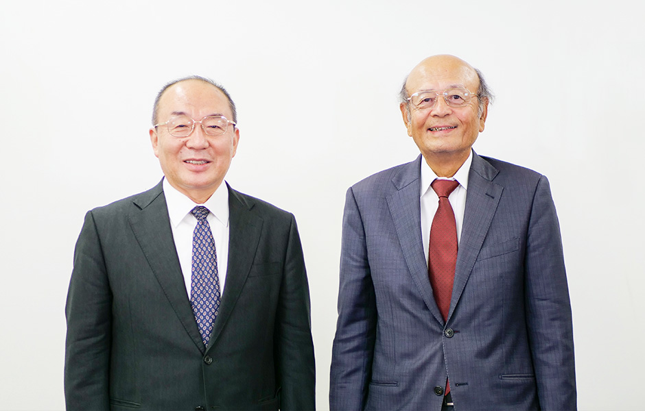
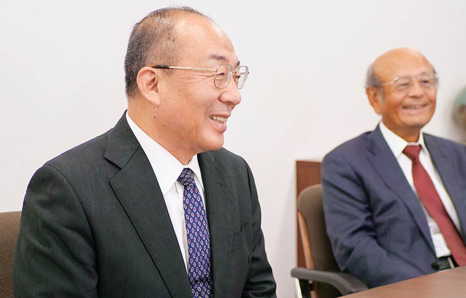
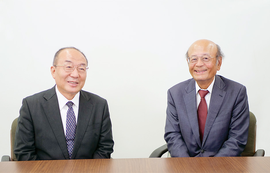
In this issue of Shareholder Communications, Yasunobu Morishima, President and Representative Director, and Ko Cho, Director and Executive Vice President, discuss the Semiconductor-related Business, which is the key to our company’s growth, the business integration process, and future outlook.
It was fate that A&D and HOLON, both pursuing the same dream, would meet.
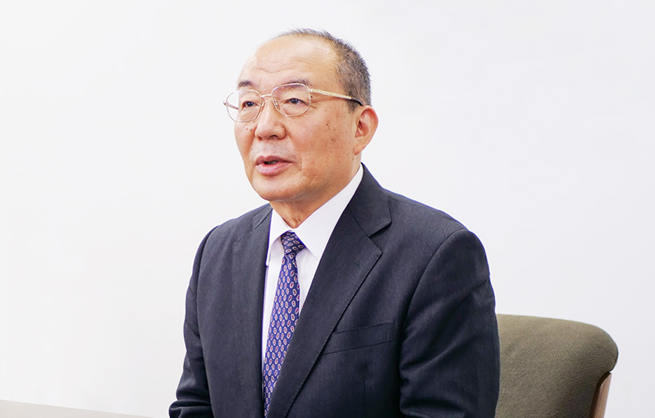
President Morishima: The predecessor to our company, A&D, was founded in 1977. The 1970s was a time of rapid growth in Japan’s semiconductor industry, when semiconductors replaced conventional vacuum tubes and became widely used in electronic devices. The telecommunications industry in particular was the driving force behind rapid innovation during those decades. At first, telephones were manually operated by a switchboard, but an automatic switchboard was introduced to automatically connect calls without human intervention. However, the automatic switchboards of the time had a short lifespan and frequently broke down.
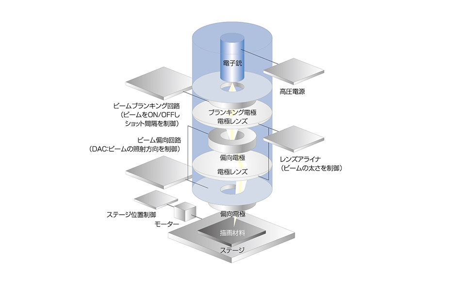
As a solution to this problem, an automatic switchboard system was developed utilizing semiconductors. Semiconductors require photomasks (templates for integrated circuits) which makes mass production of semiconductors possible. Photomasks are made from precise and accurate electron-beam mask writing systems capable of creating high-tech circuits. In the 1970s, the telecommunication equipment industry was working on such developments but lacked expertise in the electron beam technologies that perform D/A conversions to accurately irradiate electron beams onto a photomask.
So it was around this time that the telecoms asked companies with a background in electron beam knowhow to further develop this technology.
Electron Beam Lithography
A&D and HOLON were both established separately but founded by engineers that spun out from other companies working on electron beam technologies. These associates shared a passion for the hard work needed to evolve the state-of-the-art semiconductors. As they chased their dreams, the two companies were drawn closer together and have since built the cooperative relationship that we now have today. In this sense, I believe that the synergy between our two companies was not a coincidence, but inevitable and destined to happen.
The fusion of A&D and HOLON world-class technologies will trigger a new chain reaction to advance Semiconductor-related Business opportunities.
Vice President Cho: HOLON has particular expertise in the technologies that control electron beams. Using this technology, we manufacture and supply Photomask CD-SEM which plays an important role in the semiconductor manufacturing process.
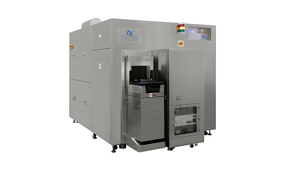
Photomask CD-SEM
CD-SEM (Critical Dimension-Scanning Electron Microscope) is a device used to measure the width of circuit patterns on semiconductor photomasks (original circuit plates) to inspect and measure whether they are correctly drawn according to design specifications. HOLON boasts world-class technology in photomask inspection and measurement equipment, which contributes to the steady performance of its Semiconductor-related Business. We expect sales of the Semiconductor-related Business to grow 18.6% in FYE March 31, 2024(forecast) compared to the previous year’s results, and we believe we can expand further in the coming year.
President Morishima: A&D originally excelled in A/D and D/A conversion technology (technology that mutually converts analog and digital). In the manufacture of semiconductor photomasks, the electron beam emitted from the electron gun must be operated with high precision and at high speed. A&D possesses the world’s highest level of accuracy and speed in controlling the direction of electron beam irradiation. One nanosecond is one billionth of a second, but the mask lithography system changes the voltage precisely in several nanoseconds, a speed unimaginable to the average person. We believe that A&D’s superiority within the lithography equipment industry lies not only in its accuracy or speed, but also in its circuit technology.
A&D also specializes in high-voltage power supply technologies, possessing analog technology that generates extremely high voltages of several tens of kilovolts. This technology also provides the associated units needed to generate the electron beam.
HOLON has unparalleled technology and expertise in handling the electron beam itself, and A&D is a world leader in controlling the direction of electron beam irradiation. Collaboration between the two companies is the greatest pairing – a technological powerhouse alliance that will greatly grow the semiconductor industry business.
Synergies generated by the A&D and HOLON business integration
President Morishima: Combining A&D’s and HOLON’s technology and expertise makes for a strong team in electron beam technology and other areas. In particular, talking from an economic security standpoint, countries around the world are seeking independence in semiconductor manufacturing and related technology development. By making good use of the sales networks and resources that each company had originally, a global structure will be established, allowing for quick response to demand in different countries and regions. Furthermore, in terms of procurement and purchasing of parts and other items, an increase in efficiency and cost effectiveness of parts procurement is expected from the increase in overall buying power.
In addition, although it is now becoming more difficult to obtain key personnel, the management integration has opened up opportunities to optimally assign engineers with advanced expertise across various fields more efficiently. As we increase synergistic effects, we hope to use these opportunities in order to speed up our research and development.
Vice President Cho: HOLON was listed on JASDAQ in 2005 (now: TSE Standard) and grew as a small company, then became an affiliate of A&D in 2008, a consolidated subsidiary in 2018, and a member of a large organization through this business integration. President Morishima is certainly a special person. We have many excellent staff members working at our company, but President Morishima possesses a particularly broad perspective to globally envision the future. In such rapidly changing times, I think this is a very important quality of a Japanese leader.
This integration not only allows us to utilize each other’s resources in terms of technological development, but also strengthens management control and human resources, allowing HOLON to focus on product development as a business subsidiary.
President Morishima: Vice President Cho has worked diligently on electron beam technology. More than an engineer, he is a marketer in the semiconductor field, and a valuable marketer at that. Surprisingly few people, including those in the semiconductor industry, understand the technology and can flexibly respond to market changes. Vice President Cho is originally a technical person, but the more I talk to him, the more I notice his marketer sense.
Market demand is for further miniaturization and multilayering. Going forward, we will seize opportunities for success for the entire group, with the Semiconductor-related Business at the core of our operations.
Vice President Cho: HOLON was doing business in Taiwan through a local distributor but has now opened a new branch office. Taiwan plays an important role in the semiconductor industry and is home to many major semiconductor manufacturers. By establishing a system that directly handles sales activities and maintenance services, we aim to achieve further growth by accurately grasping customer needs, further speeding up service response, and building a system that allows us to reflect truly needed functions in equipment development.
President Morishima: As stated in our medium-term management plan, we aim to contribute to a “digital society”, a “healthy and long-lived society”, and a “carbon-neutral society” by making even more effective use of each other’s technological capabilities and management resources. With fields such as AI and IoT rapidly increasing demand for semiconductors, we position our Semiconductor-related Business as an essential growth driver for our company’s rapid progress.
We will strive to achieve sustainable growth for the entire group centered on the growth driver of Semiconductor-related Business while contributing to solving social issues through our business activities and realizing shareholder returns that meet everyone’s expectations. We look forward to your continued support.
TOPICS
A&D HOLON Holdings and
its connection with stakeholders
A&D HOLON Holdings
Celebrates First Anniversary
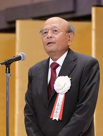
On July 12, we held the
“A&D HOLON Holdings First Anniversary Celebration – One Global A&D HOLON – ” event at the Imperial Hotel Tokyo to commemorate the first anniversary of our holdings company structure.
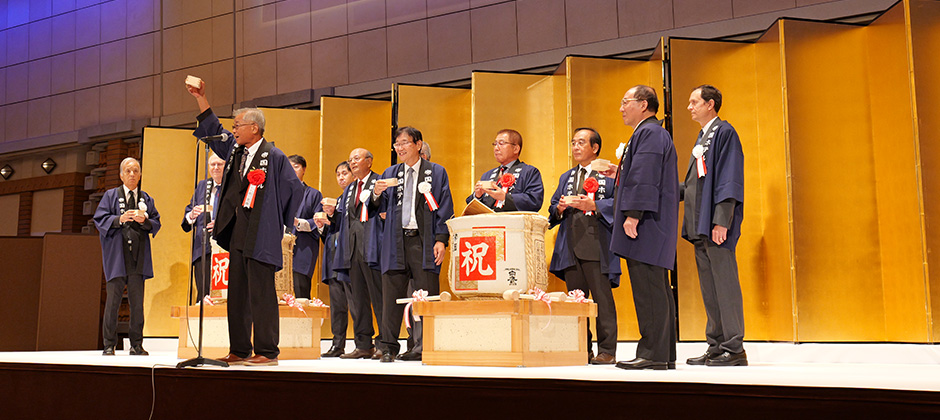
The ceremony was attended by approximately 350 guests, including business partners and alliance partners, as well as the mayor of Kitamoto City, Saitama Prefecture, where A&D’s largest business base, the Development and Technology Center, is located.
The congratulatory address included a video letter from the plant manager of the Photomask Manufacturing Division of TSMC Corporation of Taiwan, the world’s largest semiconductor manufacturer. During the ceremony, Professor Emeritus Daisho, an outside director who is also a professor emeritus at Waseda University and an advisor to the Next Generation Vehicle Research Organization Research Institute, gave a lecture on carbon neutrality.
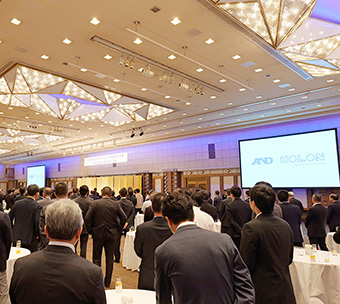
It was President Morishima’s strong desire that all employees create “handmade gifts” together and present them to the participants on the day of the event as an expression of gratitude. In addition, booths were set up at the venue to display products, videos were shown to introduce the business, and detailed explanations were provided by each person in charge of the project. One participant commented, “I didn’t know your company produced such a wide variety of products.”
* Japanese language only
Learn more about our products


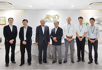
Mayor of Kitamoto City visits
A&D Development & Technology Center
On August 8, 2023, Mr. Yukio Sangu, Mayor of Kitamoto City, Saitama Prefecture, visited A&D Development and Technology Center.
This visit was arranged after a request to observe a company based in the city from the mayor, who was a guest of honor at the first anniversary celebration of A&D HOLON Holdings.
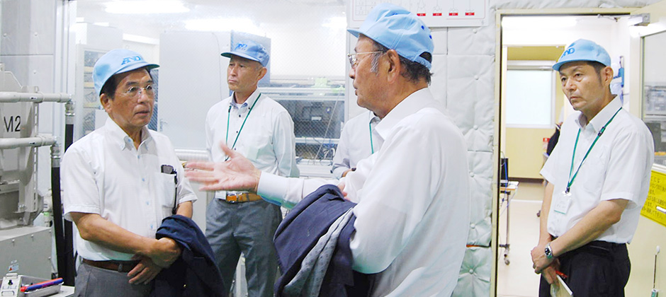
During the tour, the visitors viewed workplaces and toured tire testing machines at A&D’s Konosu Plant and engine benches in the Development and Technology Center, before chatting with President Morishima. Through the event, visitors acquired a better understanding of our company and we established further ties with Kitamoto City, and we promised to continue to strengthen ties and contribute to the community.