Semiconductor-
related Business
Making a more convenient world
The rapid digital transformation of society has drastically changed our way of life. In response to the demand for smaller and more advanced semiconductors, our business provides cutting-edge technologies for dimensional measurement and related processes, leveraging advanced electron beam technology.
Our flagship product for CD-SEM (Critical Dimension-Scanning Electron Microscope) is crucial for developing increasingly sophisticated semiconductor photomasks. These photomasks are used to create silicon chips for computers, smartphones, and digital electronics, which are becoming increasingly advanced and compact.
To keep pace with the rapidly evolving digital society, we will continue to combine world-class technologies and products. We are strengthening the collaboration between our R&D, manufacturing, sales, and support operations to meet the expectations of the industries we serve.
Strengths in semiconductor-related business
Customers
We are expanding our business with leading semiconductor manufacturers and photomask manufacturers both in Japan and overseas.
Knowledge & Technology
We adapt to recent trends in the semiconductor industry and consider the needs of our customers as they pursue cutting-edge technologies to advance the state of their industries.
Looking to the Future
In the future, IoT and AI is expected to spread into every corner of our society and lives and semiconductor-related industries will be directly correlated with this increased growth.
A&D Company, Limited and HOLON Co., Ltd. operate within the semiconductor industry.
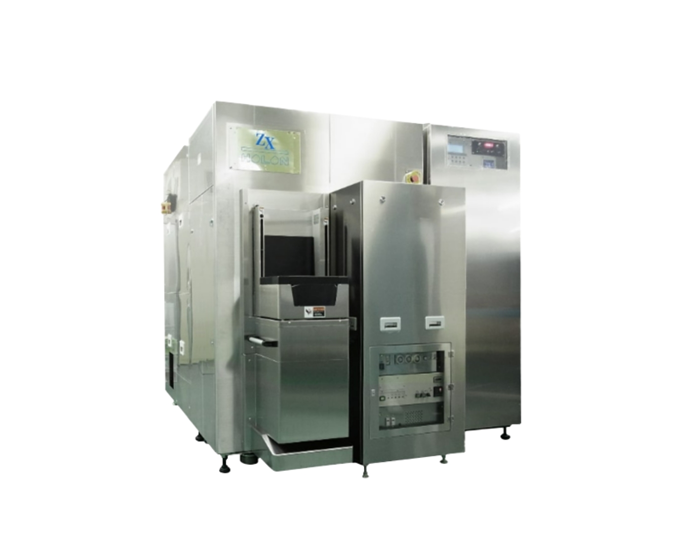
Semiconductor and Photomask Dimension Measurement Equipment
Electron beam technologies optimal for measuring the dimensions of fine circuit patterns on silicon wafers
HOLON Co., Ltd.’s product for CD-SEM (Critical Dimension-Scanning Electron Microscope) performs dimensional measurement to ensure that semiconductor photomasks, used in the manufacturing of silicon chips for devices such as personal computers, smartphones, and digital appliances, are produced accurately in accordance with design specifications.
Additionally, HOLON Co., Ltd.’s analytic tools for SEM are essential in the development of cutting-edge semiconductor manufacturing using EUV lithography.
HOLON Co., Ltd. invests in advanced research and development and is committed to providing optimum products and services to support the semiconductor and nanotechnology industries that are evolving at a rapid pace.
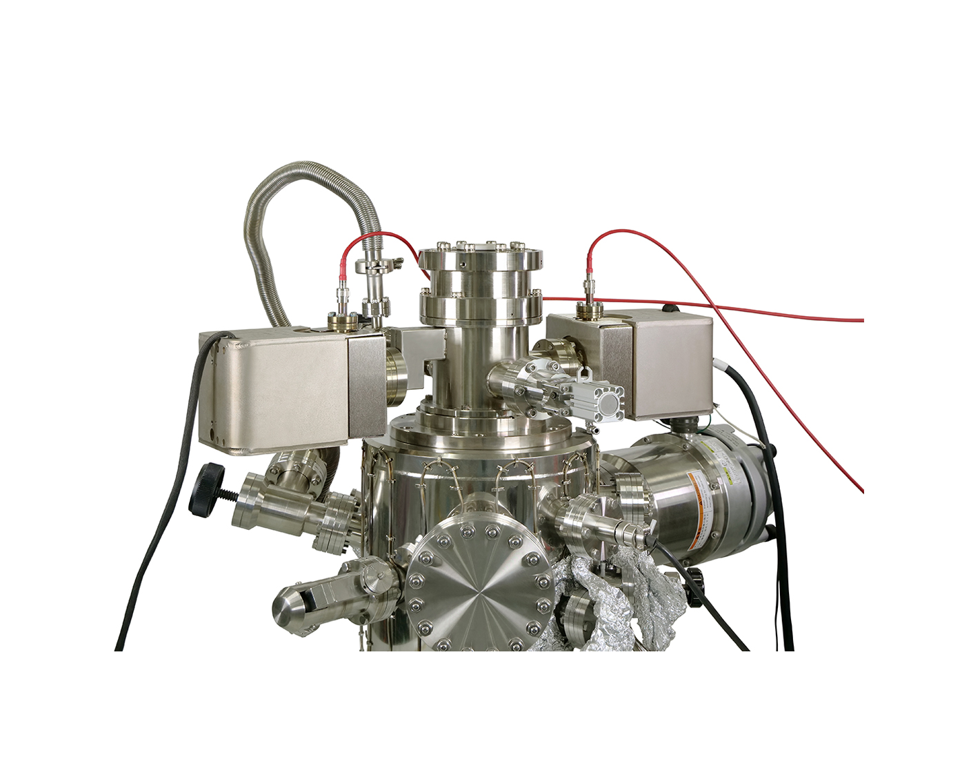
Semiconductors and Nanoelectronics Manufacture and Control
Supplying core technology for use in electron beam lithography devices
A&D Company, Limited is a pioneer in developing electron guns that generate electron beams and ships products with world-class output and stable operation rates.
These electron beams are used in applications such as electron microscopes capable of observing and measuring at the nano-scale and in electron beam fine processing equipment used in nano-scale processing.
Future development will continue to achieve further miniaturization which enables greater performance and the expansion of use-cases that will support the advancement of semiconductor and other cutting-edge industries.
Learn more about our semiconductor-related business strategy.