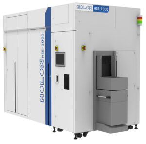
HOLON CO., LTD., a subsidiary of A&D HOLON Holdings Company, Limited, announces the release of its new product, the Next-generation Photomask CD-SEM, “HSS-1000,”
1. Overview of New Product
HSS-1000 offers significantly improved performance over the previous ZX model, achieving an extremely high CD measurement accuracy required for EUV mask manufacturing in the 1.6nm node and beyond. Furthermore, it is capable of acquiring clear, high-resolution SEM images of thin-film absorber layers and photoresist patterns. This enables significant yield improvements in mass production and increased efficiency during the mask development stage.
2. Development Background
With the full-scale introduction of EUV lithography in the wafer fabrication of cutting-edge nodes, mask patterns are rapidly becoming finer due to continuous scaling and pattern complexity. This has brought new challenges to the forefront, such as improving CD measurement accuracy, ensuring throughput, high-resolution observation of thin-film absorber layers and photoresist patterns, and detecting the edge placement of curvilinear patterns. In order to address these challenges, we have brought together the innovative technologies of our group companies to develop a new product.
3. Main Features
- Newly designed electron optical systems and aberration correction technology enable high-resolution SEM images, and significantly improves measurement accuracy of fine patterns.
- The beam control circuit has the same accuracy and speed as ones for an EB lithography system, which enables high-speed and high-precision CD measurement, strengthening its capabilities in mass production use.
- Low incident energy (100 eV) allows for low damage to photoresist patterns, enabling high-resolution measurement while suppressing resist shrinkage.
- The newly designed platform’s pallet-less transport and high-speed stage significantly improve throughput, meeting the needs for mass production.
- AI technology predicts and corrects for focus and positioning deviations of the e-beam, and De-noise processing enables higher resolution and stabilization of SEM images.
- Implementation of low vacuum technology and VUV provides powerful charging-mitigation solutions to suppress image degradation caused by charging effect and support stable measurement.
- High-precision contour extraction function enables EPE analysis for curvilinear patterns.
4. Improvements in performance compared with the previous model, ZX
- CD measurement accuracy (Static) … 25% improved
- Beam resolution (Sharpness) … 15% improved
- Contrast-to-Noise ratio (CNR) … 15% improved
- (MAM time) … 30% improved
5. Future plans
We will strengthen our development resources across all A&D HOLON holdings group companies and establish a system that can meet the needs of each customer in detail. Through introduction of the HSS-1000, we will strengthen our position in the Asian market and accelerate penetration into the EU and U.S. markets.
Contact for Inquiries
A&D HOLON Holdings Company, Limited
Public Relations and Investor Relations Section,
Corporate Planning Department
Tel: +81-3-5391-6124